Memory addressing problem
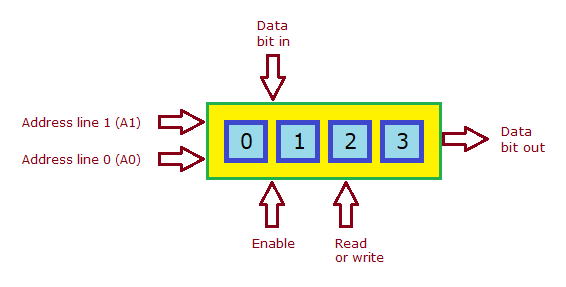
Below is a fictional RAM chip.
It has only four cells, i.e. can only store four bits, labelled below as 0,1,2, and 3.

Example operation
To write a 1 to cell 2 (bit 2):
Step 1: Put 2 on the address bus pins (A1 and A0).
Step 2: Set the 'read or write' pin to write.
Step 3: Set the 'data bit in' pin to 1.
Step 4: Set the enable pin to enable.
To later read back that cell:
Step 1: Put 2 on the address bus pins (A1 and A0).
Step 2: Set the 'read or write' pin to read.
Step 3: Set the enable pin to enable.
Step 4: Examine the 'data bit out' pin.
Inadequate testing
You might think that the following test script would be good enough to test the chip.
STEP 1: Cell 0 is target - Write the data of 0 to address 0, then verify that 0 is read back from address 0.
STEP 2: Cell 0 is target - Write the data of 1 to address 0, then verify that 1 is read back from address 0.
STEP 3: Cell 1 is target - Write the data of 0 to address 1, then verify that 0 is read back from address 1.
STEP 4: Cell 1 is target - Write the data of 1 to address 1, then verify that 1 is read back from address 1.
STEP 5: Cell 2 is target - Write the data of 0 to address 2, then verify that 0 is read back from address 2.
STEP 6: Cell 2 is target - Write the data of 1 to address 2, then verify that 1 is read back from address 2.
STEP 7: Cell 3 is target - Write the data of 0 to address 3, then verify that 0 is read back from address 3.
STEP 8: Cell 3 is target - Write the data of 1 to address 3, then verify that 1 is read back from address 3.
Example of an addressing problem
Let us pretend that the example chip has a fault that internally, results in the A1 line always being LOW.
I execute the aforementioned test script. It results in a PASS !!!
Here is what happened:
STEP 1: Cell 0 is target - 0 stored in cell 0, and read back as 0. <-- PASS
STEP 2: Cell 0 is target - 1 stored in cell 0, and read back as 1. <-- PASS
STEP 3: Cell 1 is target - 0 stored in cell 1, and read back as 0. <-- PASS
STEP 4: Cell 1 is target - 1 stored in cell 1, and read back as 1. <-- PASS
STEP 5: Cell 2 is target - Due to the addressing fault, the cell reached is cell 0, not 2. 0 stored in cell 0, and read back as 0. <-- PASS
STEP 6: Cell 2 is target - Due to the addressing fault, the cell reached is cell 0, not 2. 1 stored in cell 0, and read back as 1. <-- PASS
STEP 7: Cell 3 is target - Due to the addressing fault, the cell reached is cell 1, not 3. 0 stored in cell 1, and read back as 1. <-- PASS
STEP 8: Cell 3 is target - Due to the addressing fault, the cell reached is cell 1, not 3. 1 stored in cell 1, and read back as 1. <-- PASS
Cells 2 and 3 did not get tested.
But that is minor compared to the addressing problem, eg. writing to address 2 overwrites the data stored at address 0.
How might this problem be tested for? By verifying that a test write to each address does not affect another address.
Additional information
The motherboard (or RAM card) circuitry can also create this situation.
ROM's can be similarly affected.
